Frequency Synthesis: Engineering an AD9851 Based DDS System
By Eyobed on 8/13/2025
This post will discuss about the frequency synthesizer system I built as a part of my day Job. The system utilizes the Analog Devices AD9851 CMOS DDS core to produce numerically controlled analog waveforms. at a much better accuracy than almost any other method. I have categorized the post by section so you can have a structured reading. :)
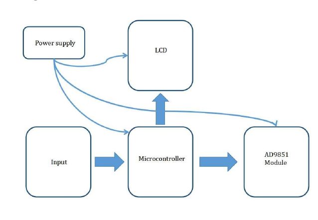
System Architecture and Component Selection
The primary design objective involved the implementation of a stable, highresolution RF source capable of precise frequency increments. that is +1Hz
Main parts:
- AD9851 Direct Digital Synthesis Core: This component from ADI features an integrated 10-bit DAC and a 32-bit frequency control word. Utilizing the internal 6x reference clock multiplier enables an internal clock speed of 180 MHz. Periodic synthesis is achievable up to approximately 70 MHz, a limit dictated by Nyquist criteria. Tested it fine until 90MHz.
- ATmega328p Controller: This unit manages serial & parallel communications with the DDS chip and executes the logic requisite for frequency to FCW translation and peripheral management.
- Interface: A 4x4 matrix keypad used for parameter entry, while a standard 16x2 character LCD provides user interface.
DDS Math
The AD9851 employs a 32-bit phase accumulator for frequency synthesis. The fundamental relationship between the desired output frequency and the frequency tuning word is governed by:
Frequency Tuning Word Calculation:
FTW = (f_desired × 2^32) / f_SYSCLK
Where:
FTW= 32-bit Frequency Tuning Wordf_desired= Target output frequency in Hzf_SYSCLK= System clock frequency = 180 MHz for AD9851 with 6x PLL enabled2^32= 4,294,967,296 constant for 32-bit accumulator
Frequency Resolution:
The minimum achievable frequency step is:
Δf = f_SYSCLK / 2^32 = 180,000,000 / 4,294,967,296 ≈ 0.0419 Hz
This sub-hertz resolution enables precise frequency control across the entire synthesis range.
Phase Control:
The AD9851 provides 5-bit phase control with 11.25° resolution:
Phase_register = ⌊desired_phase / 11.25⌋
Valid phase range: 0° to 180° in 11.25° increments.
Implementation Details
The complete implementation is available in the AD9851 GitLab repository. Key implementation aspects include:
Frequency Word Computation:
void AD9851::SetFrequency(unsigned long frequency) {
  frequencyWord = (frequency * pow2_32 * 1UL) / DDS_CLOCK;
}
Where pow2_32 = 4294967296 and DDS_CLOCK = 180000000 Hz.
Phase Word Computation:
void AD9851::SetPhase(int phase) {
  int desiredPhase = phase % 181;
  if (desiredPhase < 0)
    desiredPhase += 181;

  phaseWord = static_cast<uint8_t>((desiredPhase / 11.25));
}
Serial Loading Protocol:
The 40-bit control word structure:
- Bits 0-31: 32-bit frequency tuning word
- Bit 32: 6x PLL multiplier enable
- Bit 33: Reserved
- Bit 34: Power down control
- Bits 35-39: 5-bit phase offset word
void AD9851::LoadSerial() {
  // Load 32-bit frequency word
  for (int i = 0; i < 32; i++) {
    digitalWrite(_DATA, (frequencyWord & 0x01));
    pulseHigh(_W_CLK);
    frequencyWord >>= 1;
  }

  // Load control bits and phase
  // ... (see repository for complete implementation)

  pulseHigh(_FQ_UD);  // Update frequency
}
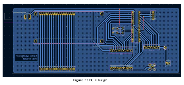
PCB Implementation and Signal Integrity
The schematic was simple so we dive straight to PCB work
Engineering Challenges:
- Custom Footprints: Due to the absence of a standard footprint for the AD9851 breakout module within the KiCad library, a custom footprint was derived via optical scaling and pin pitch verification.
- Single Layer board: To facilitate rapid prototyping, a singlelayer copper layout was utilized. Routing was optimized to minimize parasitic inductance and capacitive coupling, factors critical for maintaining signal integrity at elevated oscillator frequencies.
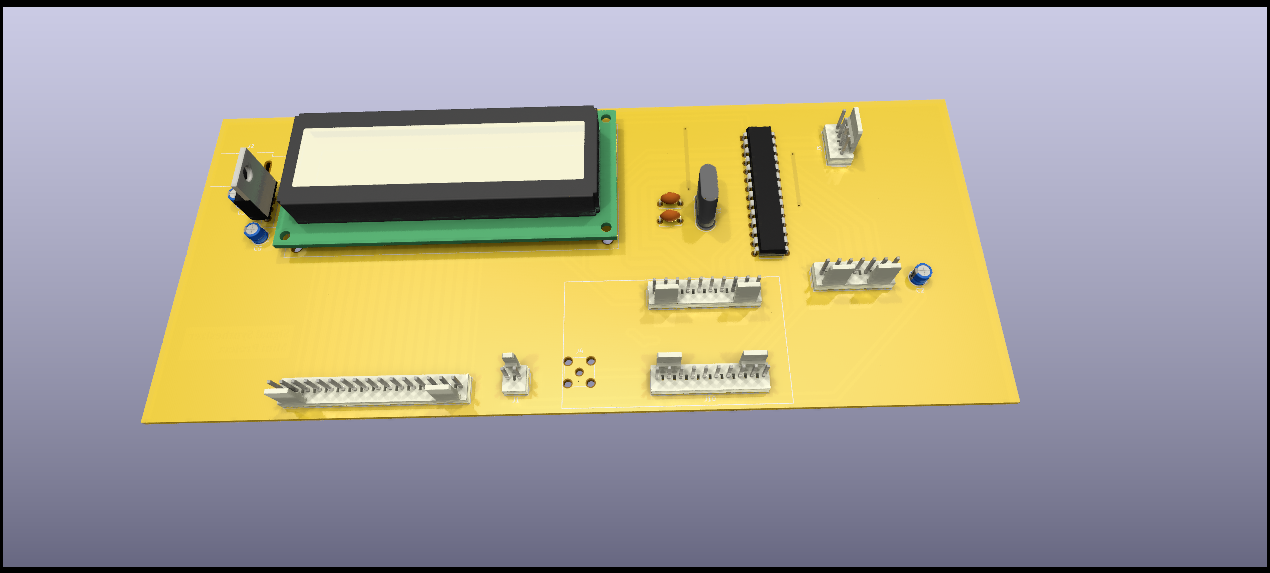
- 3D : as shown below
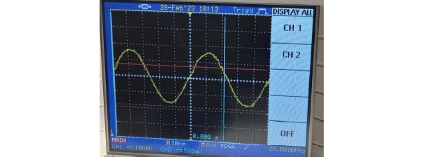
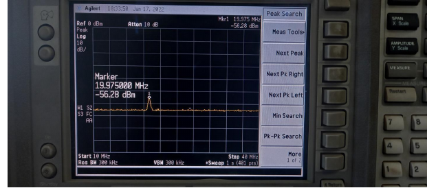
Verification and Spectral Analysis
Post-assembly validation focused on the quantification of frequency accuracy and spectral purity under varying load conditions.
**Experimental Setup: Oscilloscope **
Domain Analysis:
1. Time-Domain: The input of a 20 MHz target frequency resulted in a stable sinusoidal output with negligible phase jitter, as seen via oscilloscope capture.
2. Frequency-Domain: A spectrum analyzer was employed to evaluate the Spurious-Free Dynamic Range, and harmonic distortion.
- Single-Tone Evaluation: Under 20 MHz singletone operational parameters, the system shown a high-amplitude fundamental peak with a minimal noise floor, thereby confirming precise synthesis.
- Dynamic Sweep: A sweep from 20 MHz to 30 MHz demonstrated a linear amplitude-frequency response across the specified bandwidth, validating the reliability of the control logic and DAC performance.
Conclusion
This project successfully validates the conversion of a theoretical DDS architecture into a functional laboratory-grade instrument. Technical objectives regarding 32-bit frequency resolution and spectral stability were achieved, establishing a robust platform for subsequent RF experimentation.